Wavefunction imaging of InAs QDots
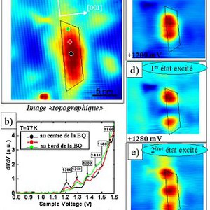
The figure illustrates our imaging and spectroscopy measurements by STM at T=77K of the quantized electronic states in InAs QDots encapsulated in GaAs. The STM image, (fig. a), shows the topography of a QDot seen on the edge of a cleaved heterostructure containing self-assembled InAs QDots, the atomic rows of the GaAs cleavage surface lattice (110) and some sub-surface dopants (bright spots). The differential conductance, dI/dV measured by tunnel spectroscopy, (fig. b), reveals the discrete spectrum of electronic states in the QDot. The differential conductance images, measured for each of the peaks, reveal in real space, the lobes and nodes of the square module of the electronic wave function, revealing respectively the symmetry s, p d of the fundamental state (fig. c) and the first two excited states (fig. d and e).
Contact:
Low temperature scanning tunneling microscopy wave-function imaging of InAs/GaAs cleaved quantum dots with similar height
J.-C. Girard, A. Lemaitre, A. Miard, C. David, and Z.Z. Wang


