Nanostructures


Superconducting parity effect across the Anderson limit

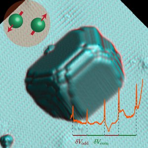
What is the minimum size for a nanocrystal to be superconducting? In 1959, P.W. Anderson suggested that superconductivity could exists only when the energy interval between electronic levels is smaller than the superconducting energy scale, i.e. the superconducting gap, which corresponds to the binding energy of the Cooper pairs responsible for superconductivity. Until now, this remained a conjecture. However, using a Scanning Tunneling Microscope (STM) to study superconducting Lead (Pb) nanocrystals grown on the 2D electron gaz at the surface of Indium Arsenide, LPEM researchers have observed that Cooper pairing disappears when this level spacing became larger than this superconducting energy scale, demonstrating the validity of the Anderson criterion. This experiment establishes a new method for investigating nanocrystals in the regime of strong quantum confinement with promising perspectives for the study of electronic orders in the chemical limit, i.e. when the electronic spectrum of a solid becomes discrete.

Contact:

Superconducting parity effect across the Anderson limit
S. Vlaic, S. Pons, T. Zhang, A. Assouline, A. Zimmers, C. David, G. Rodary, J-C Girard, D. Roditchev, and H. Aubin
Nature Com. 8 14549 (2017)


Wavefunction imaging of InAs QDots

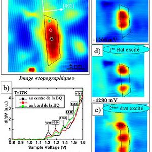
The figure illustrates our imaging and spectroscopy measurements by STM at T=77K of the quantized electronic states in InAs QDots encapsulated in GaAs. The STM image, (fig. a), shows the topography of a QDot seen on the edge of a cleaved heterostructure containing self-assembled InAs QDots, the atomic rows of the GaAs cleavage surface lattice (110) and some sub-surface dopants (bright spots). The differential conductance, dI/dV measured by tunnel spectroscopy, (fig. b), reveals the discrete spectrum of electronic states in the QDot. The differential conductance images, measured for each of the peaks, reveal in real space, the lobes and nodes of the square module of the electronic wave function, revealing respectively the symmetry s, p d of the fundamental state (fig. c) and the first two excited states (fig. d and e).

Contact:

Low temperature scanning tunneling microscopy wave-function imaging of InAs/GaAs cleaved quantum dots with similar height
J.-C. Girard, A. Lemaitre, A. Miard, C. David, and Z.Z. Wang
J. Vac. Sci. Technol. B 27(2), Mar/Apr 2009 pp891-894 (2009)


Fundings:

Logo ANR      

Publications

Quantum confinement effects in Pb nanocrystals grown on InAs
T. Zhang, S. Vlaic, S. Pons, A. Assouline, A. Zimmers, D. Roditchev, H. Aubin, G. Allan, C. Delerue,C. David, G. Rodary, and J-C. Girard
Physical Review B 97, 214514 (2018)

Superconducting parity effect across the Anderson limit
S. Vlaic, S. Pons, T. Zhang, A. Assouline, A. Zimmers, C. David, G. Rodary, J-C Girard, D. Roditchev, and H. Aubin
Nature Com. 8 14549 (2017)

Discretization of Electronic States in Large InAsP/InP Multilevel Quantum Dots Probed by Scanning Tunneling Spectroscopy
B. Fain, I. Robert-Philip, A. Beveratos, C. David, Z. Z. Wang, I. Sagnes, and J. C. Girard
Phys. Rev. Lett. 108, 126808 (2012)

Electronic structure of cleaved InAsP/InP(001) quantum dots measured by  scanning tunneling microscopy
B. Fain, J.-C. Girard, D. Elvira, C. David, G. Beaudoin, A. Beveratos, I. Robert-Philip, I. Sagnes and Z.Z. Wang 
Appl. Phys. Lett., 97 171903 (2010)

Low temperature scanning tunneling microscopy wave-function imaging of InAs/GaAs cleaved quantum dots with similar height
J.-C. Girard, A. Lemaitre, A. Miard, C. David, and Z.Z. Wang
J. Vac. Sci. Technol. B 27(2), Mar/Apr 2009 pp891-894 (2009)